Transistor Characteristic Curve
Every electronic component has their own characteristic curve. This is also true for transistors. However, unlike other electronic components which have a simple linear curve, the transistor characteristic curve has a unique linear curve depending on various variables in the circuit.
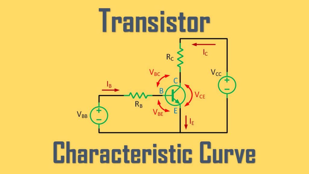
We will use an NPN transistor here in an electric circuit schematic for better learning.
Transistor Characteristics
First thing, we will find three regions in a transistor characteristic curve. They are:
- Cutoff region,
- Saturation region, and
- Active region.
The circuit consists of:
- A voltage source connected to base, VBB
- A base resistor, RB
- An NPN transistor
- A voltage source connected to collector, VCC
- A collector resistor, RC
We will use the electrical circuit below, a basic NPN transistor circuit.
From these 3 components, we will have a lot of circuit variables:
- Base voltage, VBB
- Base current, IB
- Base resistance, RB
- Base-emitter voltage, VBE
- Collector voltage, VCC
- Collector current, IC
- Collector resistance, RC
- Collector-emitter voltage, VCE
- Emitter current, IE
From the nine variables above, we will learn about the transistor characteristic curve. But do not worry, there will be only one curve with collector current (IC) and collector-emitter voltage (VCE) as the axis.
Nonetheless, those nine variables will be the foundation and reason why such a curve can be drawn so simply.
Some notable things to remember about the transistor’s three regions:
- Active region: transistor works as an amplifier,
- Cutoff region: transistor works as an open circuit, and
- Saturation region: transistor works as a closed circuit.
Before moving on to the region’s explanations, we will divide the transistor circuit into two parts.

We call the half left is the internal circuit where we can control the switching and bias of the transistor. This part only needs a small voltage source, sufficient enough to make the transistor functioning. Let’s say this part is the “control circuit” part.
The half right is the external circuit where the load is connected to the circuit. This part uses a larger voltage source to make sure the load can be energized properly. Its condition depends on the half left circuit whether the transistor is forward biased or reverse biased.
Once the base-emitter is forward biased, the external current (IC) can flow to energize the load (RC).
If you observe the electrical symbol of a transistor, you will find a little arrow in it. Just as you have guessed, it represents a diode. This is why transistors work with the principle of forward bias, reverse bias, and depletion zone (or layer).
This is the basic idea about operation of a transistor. Now let’s move on to the operation regions.
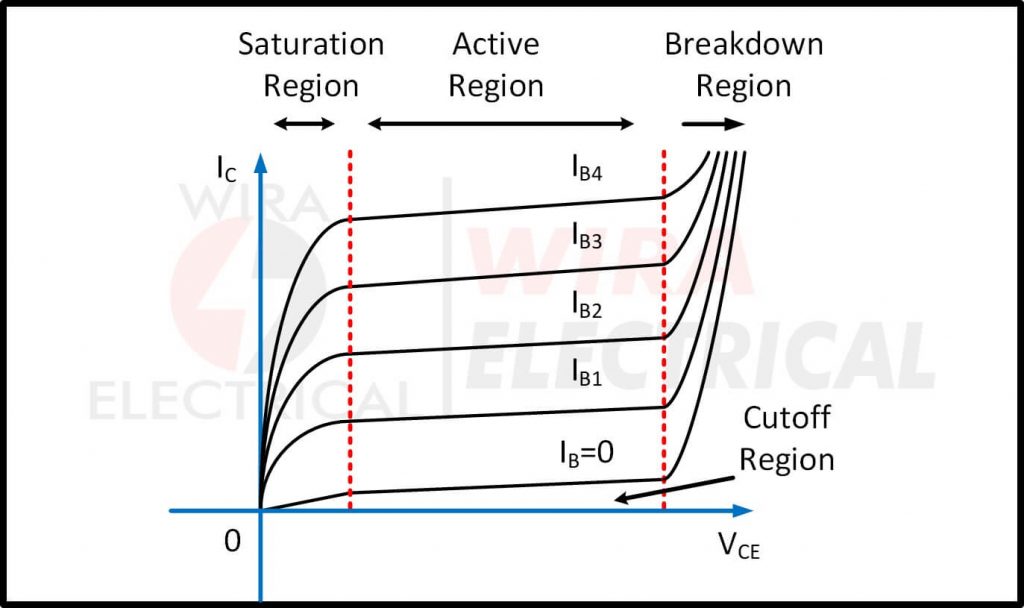
Transistor Characteristic Curve
Transistor characteristic curve is an I-V characteristic of a transistor. The vertical axis represents the collector current, IC in respect of collector-emitter voltage, VCE. Every change of collector current has something to do with collector-emitter voltage.
The transistor characteristics are divided into four regions:
- Active region,
- Saturation region,
- Cutoff region, and
- Breakdown region.
Active region is the normal operation of a transistor, where it works as an amplifier. Saturation region is when a transistor acts as a short circuit. Cutoff region is when a transistor acts as an open circuit. And last, the breakdown region is not where a transistor is supposed to work at.
Remember the curve below first and remember how it looks.
Because a transistor is capable for generating energy by amplifying the input, transistor is categorized as an active elements.
Transistor Active Region
Active region is when the transistor operates most of the time. From the curve below we can see that the line is almost perfectly horizontal straight, a bit to go up when collector-emitter voltage (VCE) is increased. This concludes that VCE affects the collector current (IC) only by little.
We can still increase the VCE before it reaches breakdown voltage value, or else it gets damaged.
Active region or linear region is achieved by increasing the collector voltage (VCC). Furthermore, increasing this voltage results in increased collector-emitter voltage (VCE). When the VCE reaches higher than 0.7 V, the base-collector terminal becomes reverse biased.
The base-collector becomes reverse biased and the base-emitter becomes forward biased. This is when the transistor works in an active region.
After the VCE is increased, it doesn’t mean the collector current (IC) is also increased. The collector current (IC) remains constant at the given value of base current (IB).
Of course there will be very small increase in collector current (IC) when VCE is increased due to the base-collector depletion region widened.
The value of collector current (IC) depends on the value of base current (IB). Therefore the collector current (IC) can be expressed mathematically by:
![]()
Where:
IC = collector current
IB = base current
ꞵ = common-emitter current gain
For more complete calculation, please refer to where we wrote about transistor analysis.
Transistor Cutoff Region
Cutoff region is when the base voltage (VBB) is zero and of course it leads to base current (IB) becoming zero. Furthermore, the PN junctions of the transistor are reverse biased resulting in collector current (IC) not able to flow.
Transistor also can’t fulfill its purpose as an amplifier in this region.
This behavior is the same with what we call an open circuit. In conclusion,
Cutoff region is when the resistor acts as an open circuit or open switch.
The collector-emitter voltage (VCE) is equal to the collector voltage (VCC) since they are in parallel where the voltage is equal no matter how big the resistance or impedance.
Transistor Saturation Region
When the collector-emitter voltage (VCE) decreases to the point it is lower than the base voltage (VB), the transistor enters the saturation region, which is nonlinear and unable to do amplification.
The saturation region can be achieved by:
- Collector voltage (VCC) is set to zero, and
- Base voltage source produces base current (IB) at a certain value.
The base current (IB) will flow through the base and emitter terminal due to the low impedance and there is current flowing through the collector, IC=0.
Furthermore, the PN junctions of the transistor are forward biased resulting in the collector current (IC) reaching its maximum value regardless of the base current (IB) value.
This behavior is the same with what we call a short circuit. In conclusion,
Saturation region is when the resistor acts as a short circuit or close switch.
The collector-emitter voltage (VCE) is zero since it is a short circuit where there is very small resistance and it can be neglected.

From the curve above, we can see that the collector current (IC) has reached its maximum value at a certain value of collector-emitter voltage (VCE) and can’t be increased further (Point B).
But increasing base current (IB) will result in increased collector current (IC) just as shown in Point B to C with the constant collector-emitter voltage (VCE).
At first, both curves will start at zero to the point A. Then they split based on the base current (IB). Higher base current will go to point B while the lower base current will go to point B.
For lower base current (IB1), the collector current (IC) starts to increase when collector-emitter voltage (VCE) is at point 1. The collector current will reach its maximum value (point B) when VCE is at point 2.
For higher base current (IB2), the collector current (IC) starts to increase when collector-emitter voltage (VCE) is at point 1. The collector current will reach its maximum value (point C) when VCE is at point 3.
Transistor Breakdown Region
We are not supposed to make a transistor work in this region. By increasing the collector voltage (VCC), the collector-emitter voltage (VCE) is also increased. Increasing this voltage leads to reverse bias on the base-collector terminal.
Increasing this further will widen the base-collector junction until it breaks. When the transistor works in the breakdown region, the collector current (IC) increases rapidly.
Conclusion
After learning about active, saturation, and cutoff regions, we can put them together in a single comparison table.
| Operation Region | Emitter Junction Bias | Collector Junction Bias | Function of Transistor |
| Active | Forward | Reverse | Amplifier |
| Cutoff | Reverse | Reverse | Switch (OFF) |
| Saturation | Forward | Forward | Switch (ON) |