
DC Transistor Circuit Analysis – Explanation and Examples
Transistor circuit analysis is a basic knowledge and skill for us electrical engineering.
A DC transistor is the most basic power electronic device with several functions.
It is very common for us to deal with electronic products on a daily basis and get some experience with personal computers.
A basic component for the integrated circuits found in these electronics and computers is the active, three-terminal device known as the transistor.
DC Transistor
You can see in Figure.(1), some various kinds of transistors are commercially available. There are two basic types of transistors: bipolar junction transistors (BJTs) and field-effect transistors (FETs).

Figure 1.
This time we will cover only the BJTs, which were the first of the two and are still used today.
Transistor Circuit Diagram
Our objective is to learn about BJTs and be able to apply the technique developed until now to analyze dc transistor circuits.

Figure 2. NPN and PNP Transistors
There are two types of BJTs: npn and pnp, with their circuit symbol as shown in Figure.(2). Each type has three terminals, designated as emitter (E), base (B), and collector (C).
The calculation below has a relationship to the transistor characteristic curve.
Transistor Circuit Analysis
For an NPN transistor, the currents and voltages of the transistor are specified as its transistor equivalent circuit in Figure.(3).

Figure 3. Transistor equivalent circuit
Applying KCL to Figure.(3a) gives
![]()
where IE, IC, and IB are emitter, collector, and base currents, respectively. Similarly, applying KVL to Figure.(3b) gives
![]()
where VCE, VEB, and VBC are collector-emitter, emitter-base, and base-collector voltages. The BJT can operate in one of three modes: active, cutoff, and saturation.
When transistors operate in the active mode, typically VBE = 0.7 V,
![]()
where α is called the common-base current gain. In Figure.(3), α denotes the fraction of electrons injected by the emitter that is collected by the collector. Also,
![]()
where β is known as the common-emitter current gain. The α and β are characteristic properties of a given transistor and assume constant values for that transistor.
Typically, α takes values in the range of 0.98 to 0.999, while β takes value in the range of 50 to 1000. From Equations.(1) to (4), it is evident that
![]()
and

These equations show that, in the active mode, the BJT can be modelled as a dependent current-controlled current source.
Thus, in circuit analysis, the dc equivalent model in Figure.(4b) may be used to replace the npn transistor in Figure.(4a).
Since β in Equation.(6) is large, a small base current controls the large current in the output circuit.
Consequently, the bipolar transistor can serve as an amplifier, producing both current gain and voltage gain.
Such amplifiers can be used to furnish a considerable amount of power to transducers such as loudspeakers or control motors.
Below is its transistor equivalent circuit.
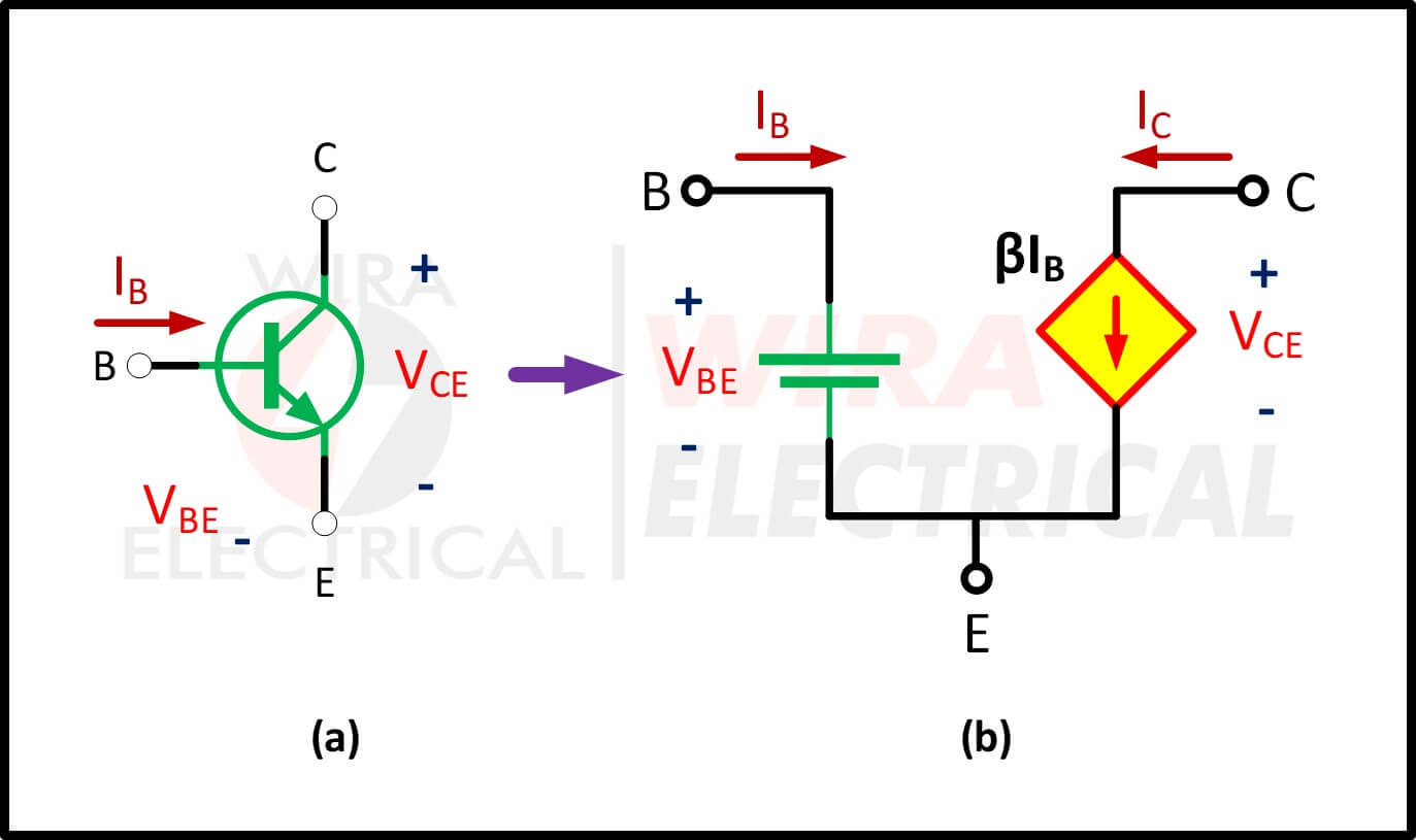
Figure 4. Transistor circuit analysis
It should be observed in the following examples that one cannot directly analyze transistor circuits using nodal analysis because of the potential difference between the terminals of the transistor.
Only when the transistor is replaced by the equivalent model can we apply nodal analysis.
DC Analysis of BJT
As mentioned above, the most common type of a DC transistor is a BJT. Now we will try to analyze it a bit before jumping to the examples and calculations.
Observe the figure below.
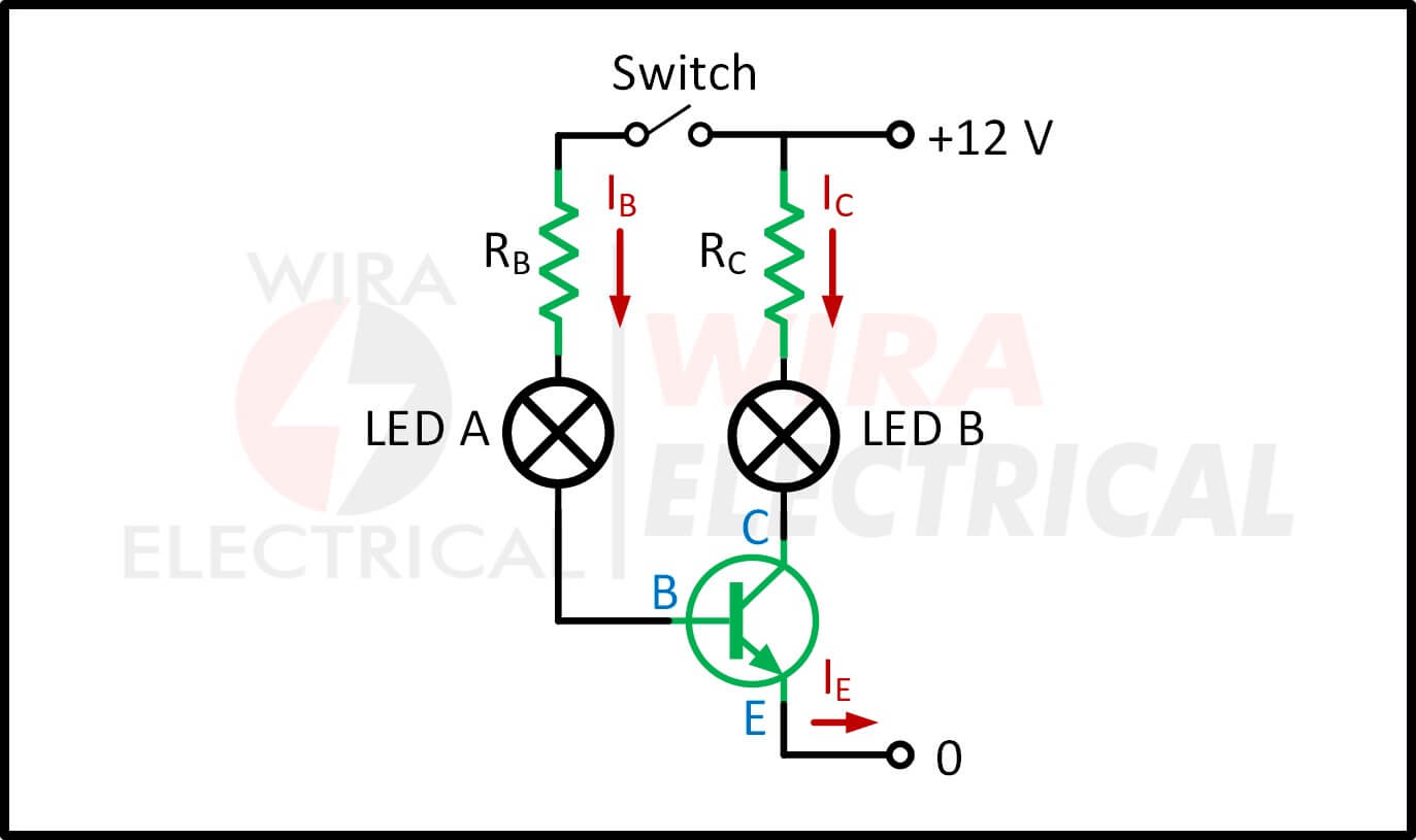
The DC transistor diagram above shows us a common emitter configuration since the emitter (E) is connected between the controlling circuit, Base (B) and the controlled circuit, Collector (C).
The base-emitter connection is the input circuit while the emitter-collector is the output circuit.
Since we only need a small portion of base current, we put higher resistance on the base (RB) and smaller resistance on the collector (RC).
This means, only with small current we will be able to control higher current.
For the initial state, the switch is open and there is no current to the base thus the transistor is not operating at the moment.
The moment we close the switch, a small current is flowing to the base (B) of the transistor and turns on the LED A dimly.
The small current to the base (base current, IB) is amplified by the transistor to allow the larger current flowing through the collector (collector current, IC) to the emitter. Since the collector current, IC is much larger, the LED B is turned on brightly.
This configuration is very common along with common-base and common-collector.
How to Solve DC Transistor Circuits
Learning how to calculate every variable in a transistor won’t help us very much when we want to use it in our circuit. We should at least understand how it works ideally.
Just as the example above shows us, we can operate it as an electrical switch.
But how so?
Observe the illustration below.

The transistor diagram above will help us in understanding how a transistor operates.
You should have seen a diode symbol when we design or analyze a circuit consists of at least one transistor.
The arrow is treated as a diode just as what we observe in the diagram above, thus
The base-emitter junction acts as a diode.
Since it is a diode, it has a forward voltage, VF of 0.7V. It means we have to at least provide 0.7V to the base-emitter junction to operate it. Then,
The base current (IB) is able to flow only when the applied voltage to the base-emitter junction (VBE) is equal or higher than 0.7V.
The small base current (IB) is able to control the higher collector current (IC) depending on the collector resistance RCE and collector voltage (VCC)
Transistor has a current gain hFE:
![]()
hFE is a constant and it has a typical value of 100 (without unit of measurement).
There are three operation modes of a transistor, they are:
- Cut off (fully off), IB = 0, then VB < VE and VB < VC
- Active, this is where a transistor operated as an amplifier and a small base current is flowing, IB > 0, then VC > VB > VE
- Saturation (fully on), base current is increased while RCE is decreased, VB > VE and VB > VC.
Looking back to the Kirchhoff’s Current Law, the emitter current is:
![]()
Since base current is much smaller than the collector current, roughly speaking
![]()
DC Transistor Circuit Analysis Examples
For better understanding, let us review the example below:
Find IC, IB, and vo in the transistor circuit of Figure.(5). Assume that the transistor operates in the active mode and that β = 50.

Figure 5. DC transistor circuit analysis example
Solution :
For the input loop, KVL gives
![]()
Since VBE = 0.7 V in the active mode,
![]()
But

For the output loop, KVL gives

Note that vo = VCE in this case.
DC Transistor Additional Notes
There are few things we should keep in mind when using a transistor, they are:
- There is a limit to the base current so we should be careful not to break it.
- Every transistor has a maximum collector current rating, check the datasheet first.
- The current gain (hFE) is widely varied even for the same type of transistor.
- When a transistor is operating at saturation mode (fully on), the RCE = 0, VCE is decreased reaching zero, and the collector current depends on the collector voltage (VCC).
The emitter current is IE = IB + IC or IE = IC since IB is very small thus make it negligible.


Thanks for the tutorial! I have to use this for my next lab report, and this was very usefull!