Common drain amplifier is also known as a source follower. This amplifier configuration has high input resistance, low output resistance, and gain approaches unity (1). You will find how we get this value below.
Common Drain Amplifier
Common drain amplifier is one of the three fundamental configurations of a single MOSFET amplifier along with common gate amplifier and common source amplifier. We will give our input voltage (Vin) to the gate and take the output (Vout) at the source where we also add a resistor on the source.

Like always, we seek for the values of:
- Input resistance (Rin)
- Output resistance (Rout)
- Voltage gain (AV)
Calculating these three will help us understand what we will get whenever we use this configuration in various circuits. Finding the value of Rin, Rout, and AV will show us how this amplifier interacts with the rest of the circuit.
First we will calculate the input resistance (Rin) by applying our test voltage source Vtest to the gate and measure the test current (itest) flowing out of it.

And its small signal model is

But looking at the model, the gate and source are separated by air gap, thus there is no current flowing through the gate. Actually, it is not completely zero but a very small number in mA but we can neglect it.

The input resistance is

The very large input resistance is the same with the common source amplifier which makes this easy to analyze further.
Next is the voltage gain (AV).
First we need to verify the value of
![]()
We use another small signal model for this case. We connect the input voltage Vin to the gate. Like the MOSFET configuration above, we connect the source to a resistor (Rs) along with its ground. The drain is connected to the VDD.
Remember that any constant voltage is represented by a ground in a small signal model since its value doesn’t change overtime. Thus, our small signal model this time is

So, what is the value of output voltage Vout?
The current is flowing from the dependent current source gmVgs to the source resistor (Rs). Hence, the voltage drop across the Rs is equal to the current times the resistance as shown below.

The Vout can be expressed by
![]()
The equation above produces another problem: what is the value of Vgs?
Classic answer, Vgs is equal to
![]()
The gate voltage (Vg) is equal to the input voltage (Vin) we apply to the gate. As a parallel connection, the voltage at the source is equal to the voltage at the output, so Vs is equal to the Vout.
Thus,

We rewrite the Vout equation into

If we put out the Vout to one side and Vin to the other side, we get

Assume that the gmRs is very large (infinite) then

The voltage gain approaches 1 (unity).
From the value of the voltage gain, this common drain amplifier acts good as a buffer.
This is why a common drain amplifier is also known as source follower. So if we are in need of an amplifier with the gain of 1, we might consider using this amplifier.

Our last calculation is to calculate the output resistance Rout.
Start with the small signal model.

Since we want to know the output resistance Rout, we will place the Vtest voltage source at the output side and calculate the current itest. All the independent sources will also be short-circuited.

We assign nodes to the intersection and apply the Kirchhoff Current Law.

Our KCL equation will be
![]()
Next we try to find the value of Vgs. The Vg is zero since the gate is connected to the ground and Vs is equal to the Vtest.

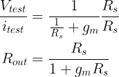
Substitute this value to the itest equation and we get

Multiplying both upper and bottom sides with Rs for better equation.

Looking back at our talk above, since this amplifier is a buffer, the gmRs will be very large (infinite), thus

The output resistance Rout is very small.
Remember from our calculations above, the input resistance is very large while the output resistance is very small.
Thus, we draw our equivalent circuit of this common drain amplifier as
