Termination Resistor – How to Use and Calculation
What is a termination resistor?
Basically, a termination resistor is a resistor placed at the end of an electrical transmission line
Why Do We Need a Termination Resistor?
Conductor is the main factor for delivering electrical signal, may it voltage, current, or digital signal.
When the length of a conductor is at least 1/6 the space filled by the up/down edges during propagation, digital signals exhibit transmission line phenomena like reflections.
In order to prevent and manage reflections in digital transmission cables, termination must be put into practice.
There are two types of termination resistor:
- Source (driver) termination
- Load (receiver) termination
By connecting a series resistor to the source resistance, which when combined with the source resistance equals the characteristic impedance of the transmission line, source disconnection prevents waves moving at the source from reflecting back to the receiver.
Source Termination Resistor
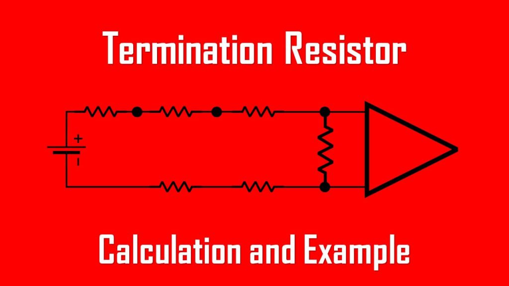
To help you understand better and easier, observe the driver circuit below
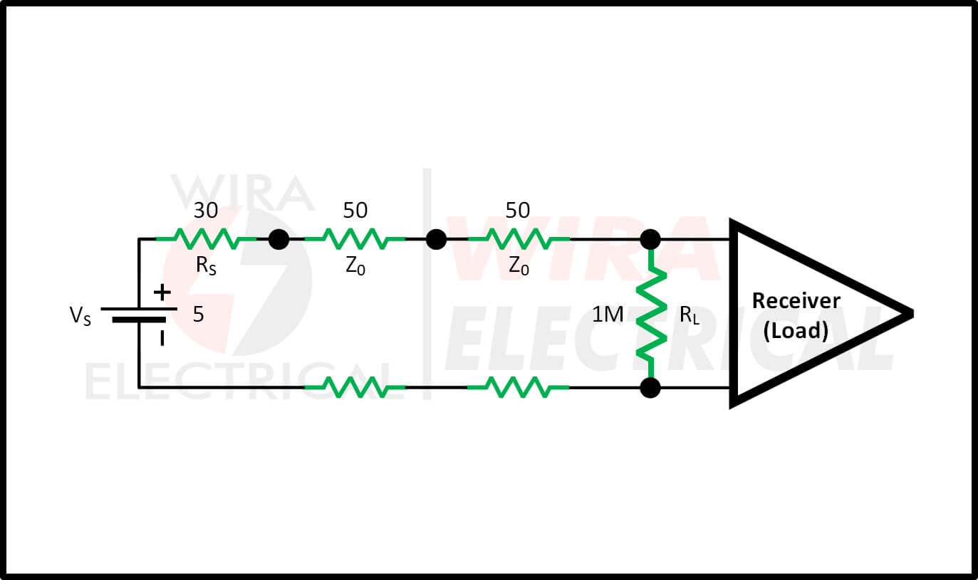
Assume that you have a driver to drive a transmission line as drawn above. From that circuit we have:
- Source resistance, RS equal to 30 Ω
- Characteristic impedance, Z0 equal to 50 Ω to the left and right of its midpoint
- Source voltage, VS equal to 5 V
- Load resistance, RL equal to 1 MΩ
If we want to terminate the signal reflection, we should use a source termination resistor (RT) at the source side.
The next question, how high the resistance we should place? Our aim is to produce equal resistance to the characteristic impedance which is 50 Ω.
We can easily calculate our termination resistor in series with a basic mathematic below:

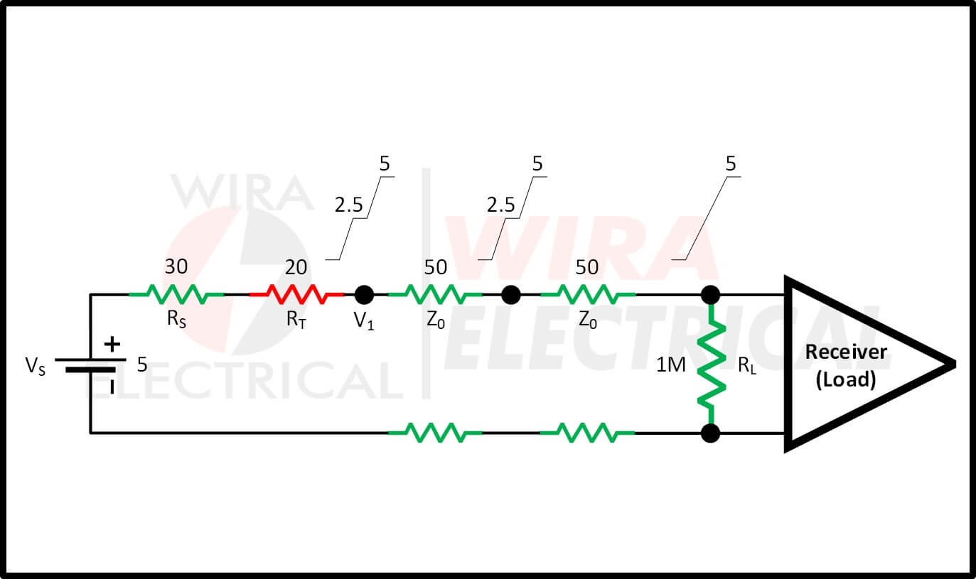
The electrical signal will first passing from the source through the voltage divider of (RS + RT) and characteristic impedance (Z0) thus the voltage at the middle of them is

This 1V voltage is what we call an “incident wave”
Incident wave is the wave flowing from the source to the receiver while reflected wave is the wave flowing from the receiver to the source.
After that, the incident wave continues to flow through the rest of the transmission line that has mismatched and high impedance. This mismatch and high impedance cause the reflection wave to travel back to the source.
Because the load resistance is much higher than the impedance of the transmission line, there will be a positive magnitude reflection wave.
Load Reflection Coefficient
The reflection wave value is
![]()
Approximately the magnitude can be said to be equal to 1.
As we have calculated above, the incident wave has the magnitude of 0.5VS and also the reflected wave has the equal magnitude.
The receiver of our driver receives the transmitted wave which consists of the sum of the incident wave and the reflected wave (0.5VS + 0.5VS = VS) without time delay between.
The slew rate of the receiver is twice of the incident edge rate, thus the voltage received is seen as twice the incident wave with the same time interval.
Why does the receiver see the twice voltage of both incident wave and edge rate?
After learning about the reflected wave and incident wave, it is better to fully understand the flow of our signal wave here.
The reflected wave which is produced by the load travels back toward the source (driver). When it reaches the source, the wave hits the RS and RT.
Just for a reminder, these resistors RS + RT serve as a Thevenin equivalent resistance. The Thevenin resistance is equal to the characteristic resistance of the transmission line.
Since those resistances are equal, the magnitude of the voltage signals are equal. Two equal waves hitting each other eliminates the bouncing phenomenon between source and load. The bounces are terminated at the source after its one back way trip.
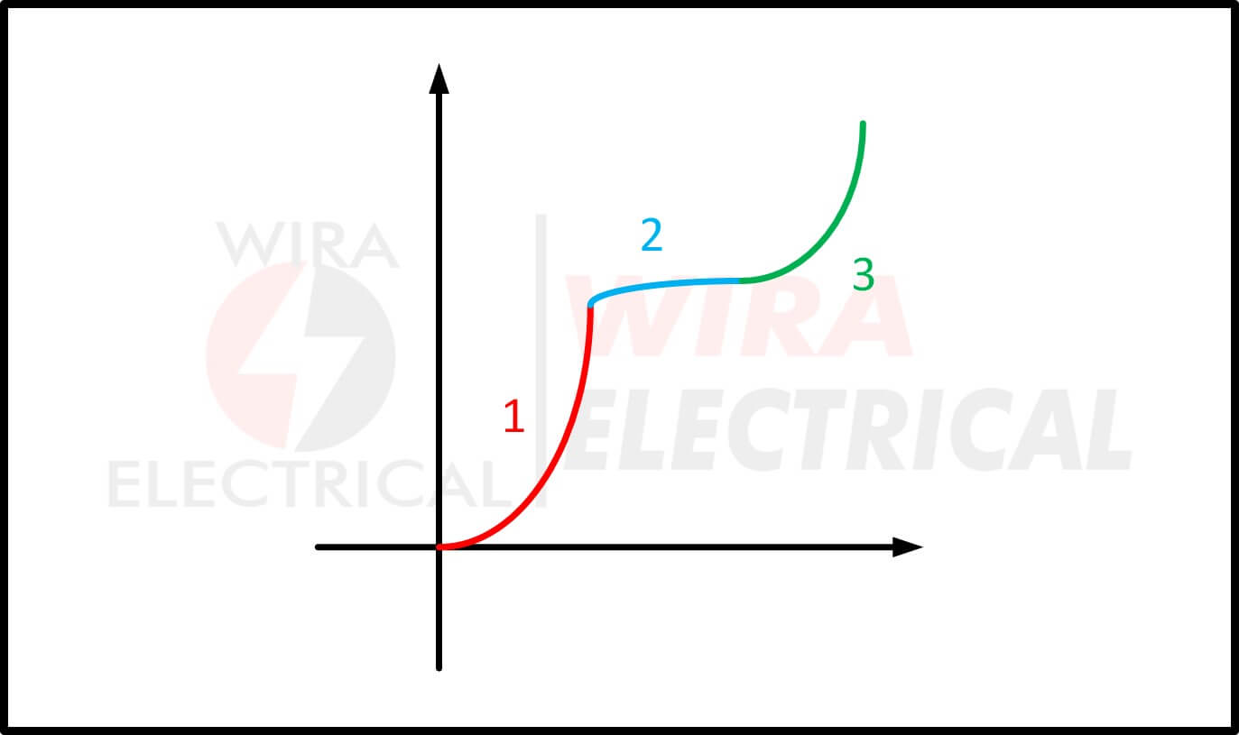
Reflected and incident waveforms
At the receiver, the received signal has a smooth curve of the full voltage equal to the source. Since there are midpoint resistors, the waveform consists of three points:
- Incident wave from 0V to 0.5VS
- Reflected wave towards the source
- Increased voltage (full voltage) to VS
The reflected wave causes the waveform to have a quick step down then quickly rises to VS.
Load Termination Resistor
There is a disadvantage of source termination resistors, that is it will have a smooth waveform if the signal is not a discrete signal or logic signal (0 and 1). The synchronous signal that is sampled by a clock signal has more varieties of magnitude compared to the logic signal.
For example, when the reflected wave is a synchronous signal it will go up to 2.5V then go down between 2.25 to 2.5 and rise to 5V.
But things will go differently with a logic signal. Just a reminder, the logic signal only knows 0 and 1. Assume that the “1” is 1V, any voltage below 1V will be treated as “0”.
The complete wave signal sequence will be:
- Incident wave from 0 to 1
- Reflected wave towards the source, 1 to 0
- Increased voltage (full voltage), 0 to 1
Thus, the sequence is 0 -> 1 -> 0 ->1.
In conclusion,
The source termination only has a good wave signal at the receiver (end of transmission line).
We can overcome this disadvantage by using the load termination resistor.
Observe the same circuit as above but with the load termination resistor instead of a source termination resistor.

Here we have a 1V voltage source that flows through the voltage divider of RS and Z0. The first generated signal VS divided by the voltage divider into:
![]()

The incident wave flows through the transmission line undisturbed until it reaches the load where the Thevenin equivalent resistance in parallel of 50Ω acts as the load termination resistor. The total resistance at the load is the parallel equivalent RT//RL.
There is no reflected wave flowing back to the source thus the wave has the same edge at every point with the same voltage and slew rate.
This configuration works very well for multiple receivers.
Since there is an advantage, there should be a disadvantage.
The load termination resistor dissipates more power thus we need higher current sourcing capacity. The power from the load is transferred to the ground and dissipates a lot of power compared to the source terminating resistor which only dissipates power when signal transition occurs.
How much of the power dissipated is caused by the load terminating resistor?
The resistor RT will dissipate
![]()
Thus we need the current source at least more than 14mW.
We can overcome this disadvantage by using the load termination resistor.
Observe the same circuit as above but with the load termination resistor instead of a source termination resistor.